How Co-Packaged Optics (CPO) Aims to Overcome the Bandwidth, Power, and Connectivity Limits?

  • Home
  • How Co-Packaged Optics (CPO) Aims to Overcome the Bandwidth, Power, and Connectivity Limits?
Patent Intelligence Report  ·  Advanced Optical Interconnect Series

How Co-Packaged Optics (CPO) Aims to Overcome the Bandwidth, Power, and Connectivity Limits of Traditional Electrical Interconnects

A data-grounded look at who is filing, where innovation is concentrated, and why it is becoming critical for next-generation AI, cloud, and HPC infrastructure.

A comprehensive technology and patent intelligence analysis of CPO — examining co-packaged optical engine integration, silicon photonics, advanced packaging, fiber-coupling technologies, and the evolving IP landscape across AI clusters, hyperscale data centers, cloud networking, HPC systems, and next-generation switching architectures.

1.6T+Data rate beyond pluggables
SiliconPhotonics integration
Co-packagedOptical engine + switch ASIC
10-partPatent landscape analysis

Report details

Co-Packaged Optics (CPO) — Technology & Patent Intelligence Report

Publisher Scintillation Research
Technology Co-Packaged Optics (CPO)
Top assignee Intel
Leading players Intel, ZTE, NVIDIA, Teramount, AlphET
IP coverage 10-part patent landscape
Applications AI, hyperscale, cloud, HPC, telecom
Audience IP, R&D, Strategy, Investment
CPO Co-packaged optics
1.6T+ Per-port bandwidth
SiPh Silicon photonics platform
IP 10-part patent analysis
360° Ecosystem coverage
Introduction

When pluggable optics can no longer keep up with AI and cloud bandwidth demands

The global Co-Packaged Optics industry is evolving rapidly as demand grows for AI clusters, hyperscale data centers, high-performance computing systems, and next-generation network infrastructure capable of supporting unprecedented bandwidth requirements.

AI training and inference workloads, cloud-scale computing platforms, and ultra-high-speed switching architectures all require interconnect solutions that deliver higher bandwidth, lower latency, and improved energy efficiency. Conventional pluggable optical transceivers continue to face limitations in power consumption, signal integrity, port density, and scalability as data rates advance toward 1.6T and beyond. The electrical signal path between a switch ASIC and a pluggable module — even at distances of centimeters — introduces signal integrity losses, SerDes power overhead, and thermal constraints that become prohibitive at next-generation data rates.

To address these challenges, the industry is developing co-packaged optics technologies that integrate optical engines directly with switching and computing silicon. Unlike traditional pluggable architectures, CPO systems reduce electrical transmission distances to millimeters, improve bandwidth density while lowering overall power requirements, and enable the port density required by future AI and cloud switching architectures.

The patent landscape is led by Intel, followed by ZTE, NVIDIA, Teramount, and AlphET. Strong contributions also come from Corning, Marvell Technology, Juniper Networks, Semiconductor Energy Laboratory, TSMC, and Optalysys — highlighting the growing role of semiconductor manufacturers, networking companies, photonics specialists, and advanced packaging innovators in advancing next-generation optical interconnect technologies.

Report structure

Table of contents

Ten chapters connecting CPO's technical foundations to patent landscape intelligence and commercialization strategy. Click any chapter to expand.

Condensed findings on CPO technology, top patent assignees, filing trends, competitive dynamics, and strategic implications for AI infrastructure, cloud networking, and optical interconnect IP
2.1 Who Will Benefit from This Report — optical interconnect engineers, network architects, IP counsel, AI hardware teams, hyperscaler infrastructure strategists, and photonics investors
3.1 Challenges in Co-Packaged Optics (CPO) — power consumption at 1.6T+, signal integrity in pluggable modules, port density constraints, SerDes overhead, fiber coupling complexity, and manufacturing integration challenges
Structural components — switch ASIC co-packaging, optical engines, silicon photonics die, fiber-to-chip coupling, modulators, detectors, and advanced packaging substrates
4.1 Key Features — ultra-short electrical reach, reduced SerDes power, higher port density, improved signal integrity at 1.6T+, thermal management, and silicon photonics integration
4.2 Problems CPO Aims to Solve — pluggable power walls, signal integrity degradation, bandwidth density limits, port count scaling, and overall data center network power budget
4.3 Potential Applications — AI training clusters, hyperscale data center switching, cloud fabric interconnect, HPC, 5G/6G fronthaul, and next-generation telecom infrastructure
CPO deployment timeline, hyperscaler adoption roadmap, OIF standardization progress, manufacturing ecosystem maturity, and near-term commercial opportunities at 800G and 1.6T
6.1 Methodology & Scope — patent database coverage, search strategy, classification framework, and analytical approach for CPO and silicon photonics interconnect IP
6.2 Scope Corrections — refinements addressing classification overlap between CPO, pluggable optics, silicon photonics, and advanced packaging patent domains
6.3 Top Assignee Picture — leading filers: Intel, ZTE, NVIDIA, Teramount, AlphET, Corning, Marvell, Juniper, TSMC, Optalysys, and Semiconductor Energy Laboratory
6.4 Notable Assignee Profiles — detailed analysis of leading assignees' CPO IP strategies, portfolio focus, and competitive positioning
6.5 Filing Activity Over Time — trend analysis identifying R&D acceleration and IP maturity signals in CPO technology domains
6.6 Jurisdiction Coverage — USPTO, CNIPA, KIPO, JPO, EPO, WIPO, and TIPO distributions across the CPO patent landscape
6.7 Technology Segmentation — patents mapped to optical engines, silicon photonics, fiber coupling, modulators, detectors, packaging, thermal management, and system integration
6.8 Foundational Anchor Patents — core IP defining the CPO landscape and their strategic competitive significance
6.9 Representative Publications Across the Field — key academic and industry publications shaping CPO research direction and deployment
6.10 Whitespace & Strategic Opportunities — unprotected technology domains and emerging filing opportunities across the CPO IP ecosystem
Stakeholder-specific takeaways for optical interconnect engineers, AI hardware teams, IP counsel, data center architects, networking equipment vendors, and photonics investors
Synthesis of CPO's technical trajectory, IP landscape dynamics, and strategic implications for next-generation AI, cloud, and HPC interconnect infrastructure
Publisher profile, research methodology, and service overview — patent analytics, technology scouting, competitive intelligence, and strategic research
Full legal disclaimer covering information accuracy, IP ownership, and terms of use for this intelligence report
Inside Co-Packaged Optics

Structural components & key features

CPO integrates optical engines directly alongside switch ASICs or compute silicon — collapsing the electrical interconnect path from centimeters to millimeters and fundamentally changing the power and bandwidth economics of high-speed networking.

Optical engine co-packaging
Silicon photonics or InP optical engines co-packaged on the same substrate as the switch ASIC — reducing the electrical signal path from centimeters (pluggable) to millimeters, eliminating SerDes signal-integrity losses.
Silicon photonics integration
CMOS-compatible silicon photonics platforms enabling monolithic or heterogeneous integration of modulators, waveguides, photodetectors, and optical multiplexers on silicon — manufactureable at standard semiconductor foundries.
Advanced fiber-to-chip coupling
Edge coupling, grating coupler, and mode converter technologies enabling efficient, low-loss optical fiber attachment to photonic integrated circuits at the chip edge — a critical manufacturing and reliability challenge for CPO.
Reduced SerDes power overhead
By shortening the electrical reach to millimeters, CPO eliminates the high-power SerDes (serializer/deserializer) stages required to drive signals across the centimeter-scale PCB traces in pluggable architectures — cutting per-port power by 30–50%.
Higher port density
Eliminating the cage mechanism and front-panel real estate of pluggable transceivers enables dramatically higher port counts per switch linecard — essential for next-generation 51.2T and beyond switch ASICs.
Thermal management innovations
Advanced thermal solutions managing the combined heat output of co-located switch ASIC and optical engine — including microfluidic cooling, thermal interface materials, and heat-spreading architectures specific to CPO packages.
Advanced packaging substrates
Multi-chip module (MCM), 2.5D interposer, and fan-out packaging architectures that co-locate optical and electronic dies with the precision alignment and thermal management required for production CPO assemblies.
1.6T and beyond bandwidth
CPO's elimination of pluggable signal integrity bottlenecks enables per-port data rates of 1.6T and beyond — supporting the next generation of AI training fabric and cloud switching architectures where pluggables cannot scale.
Challenges addressed

Why conventional pluggable optics cannot scale to AI and cloud demands

CPO directly targets five structural constraints that prevent conventional pluggable optical transceiver architectures from meeting the bandwidth, power, and density requirements of next-generation AI and hyperscale infrastructure.
01
Power consumption at 1.6T and beyond
Pluggable transceivers require high-power SerDes to drive electrical signals across PCB traces to the module cage — consuming 15–20W per port at current rates and scaling unsustainably. CPO eliminates long-reach electrical traces, reducing per-port power by 30–50% at 1.6T data rates
Power
02
Signal integrity degradation at high data rates
Electrical signal quality degrades exponentially with trace length and data rate — creating eye-closure and BER challenges that demand increasingly complex and power-hungry equalization. CPO's millimeter-scale electrical path eliminates the source of signal integrity degradation before it begins
Signal
03
Port density constraints from pluggable cages
QSFP-DD and OSFP cage mechanisms consume significant front-panel real estate, limiting port counts per switching linecard. CPO integrates optical connections at the chip edge without front-panel cages — enabling the higher port densities required by 51.2T and future switch ASICs for AI fabric topologies
Density
04
Bandwidth scalability with AI cluster growth
AI training clusters require all-to-all high-bandwidth connectivity between thousands of accelerators — creating bandwidth demands that scale quadratically with cluster size. CPO's integration of optical I/O directly with GPU and switch silicon enables the bandwidth density per chip area required for next-generation AI fabric architectures
Bandwidth
05
Data center network power budget
Network interconnect power now represents 10–20% of data center total power at hyperscale operators — and is growing faster than compute power. CPO's per-port power reduction directly reduces the fraction of data center power budget consumed by optical interconnects, improving overall PUE for AI and cloud operators
Efficiency
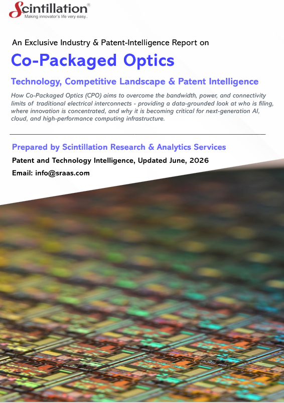
Co-Packaged Optics report cover

Request Your Sample Report Now!

    For a quick demo, schedule a meeting now!

    Shopping Cart (0 items)

    Subscribe to our newsletter

    Sign up to receive latest news, updates, promotions, and special offers delivered directly to your inbox.
    No, thanks
    Select your currency