Backside Power Delivery Network

  • Home
  • Backside Power Delivery Network
Patent & Innovation Landscape Analysis  ·  Advanced Semiconductor Series

Powering Chips From the Back: How Backside Power Delivery Network (BSPDN) Technology Is Enabling the Next Wave of Semiconductor Scaling

A data-grounded look at who is patenting, where innovation is concentrated, and what it means for IP strategy, licensing, and competitive positioning in advanced logic nodes.

BSPDNBackside power routing
GAA / CFETTransistor co-optimization
IR dropPower integrity gains
PatentLandscape & whitespace

Report details

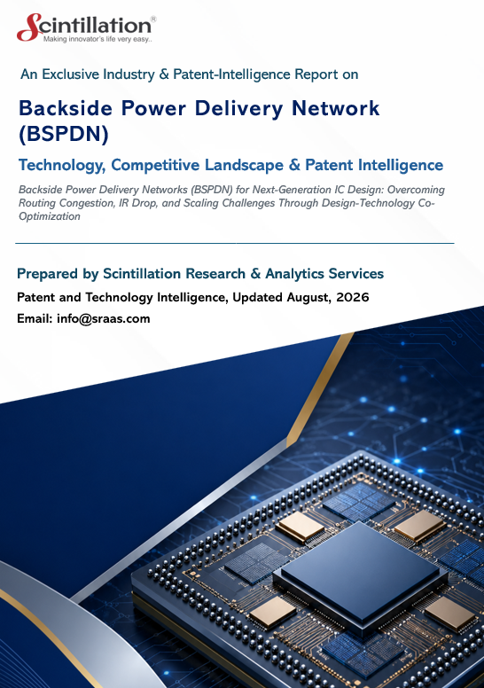
Backside Power Delivery Network (BSPDN) — Patent & Innovation Landscape Analysis Report

PublisherScintillation Research
TechnologyBackside Power Delivery Network
Focus areaAdvanced semiconductor power delivery
Key segmentsBuried Rails, TSVs, Backside Metal, GAA/CFET
IP coverage9-part patent landscape
AudienceIP, R&D, Foundries, Investment
Purpose of the report

Technology advances and IP strategy for BSPDN

This report examines the technological advances and IP landscape of Backside Power Delivery Network (BSPDN) technology, covering backside power routing, buried power rails, wafer backside processing, through-silicon vias, backside metallization, advanced transistor architectures, power and signal integrity, thermal management, and co-optimization with gate-all-around (GAA) and complementary FET (CFET) technologies for next-generation AI processors, HPC devices, and advanced nodes.

It also explores the BSPDN roadmap, manufacturing challenges, patent landscape, competitive ecosystem, and commercialization outlook across AI accelerators, data centers, HPC, mobile, networking, automotive, and edge AI, showing how BSPDN is expected to improve power delivery efficiency, reduce IR drop and power noise, raise transistor density, and support continued scaling.

Who will benefit from this report

Built for everyone shaping advanced chip manufacturing

Each audience gets a clear view of the landscape and what to do with it.

01
Patent Attorneys, Agents & IP Analysts
Filing trends, technology clusters, innovation hotspots, and whitespace to support patentability, FTO, and portfolio development.
02
Licensing & Business Development
High-value patent areas, emerging licensing opportunities, and strategic partnerships around BSPDN.
03
In-house IP, Innovation & R&D Leaders
Competitive intelligence on technology leadership, research directions, and positioning in advanced chip manufacturing.
04
Investors & Market Analysts
Visibility into commercialization readiness, industry adoption, and competitive developments in HPC and AI hardware.
05
Semiconductor & AI Chip Ecosystem
Manufacturers, foundries, EDA providers, equipment suppliers, and AI chip developers gain insight into process integration, design methods, power integrity, and roadmaps.
Introduction

Moving power wiring to the other side of the wafer

In conventional chips, power and signal wires share the same stack of metal layers above the transistors, competing for space. Backside power delivery separates them: power is routed through the back of the wafer to the transistors, leaving the front side for signals. The result can be lower voltage drop, cleaner power, and denser, less congested routing, which is why BSPDN is seen as an important enabler for advanced nodes, though it brings new challenges in wafer thinning, bonding, alignment, and heat removal.

Report structure

Table of contents

Ten chapters, from BSPDN fundamentals to patent landscape intelligence. Click any chapter to expand.

—Key findings on BSPDN technology, leading assignees, filing trends, and strategic implications
—Who Will Benefit from This Report
3.1Challenges in Conventional Backside Power Delivery Network (BSPDN)
4.1Key Features
4.2Problems Backside Power Delivery Network (BSPDN) Aims to Solve
4.3Potential Applications
—Technology roadmap, manufacturing readiness, and the commercialization outlook
6.1Methodology & Scope
6.2Scope Corrections
6.3Revised Assignee Picture
—Notable Assignee Profiles
6.4Filing Activity Over Time
6.5Jurisdiction Coverage
6.6Technology Segmentation
6.7Foundational Anchor Patents
6.8Representative Publications Across the Field
6.9Whitespace & Strategic Opportunities
—Stakeholder-specific takeaways for IP teams, licensing professionals, R&D leaders, investors, and the chip ecosystem
—Synthesis of the technical trajectory, IP dynamics, and strategic implications
—Overview of Scintillation Research and its patent and technology intelligence services
—Legal disclaimer covering information accuracy, IP ownership, and terms of use
Key features

Core technologies behind BSPDN

The building blocks that move power to the back of the wafer.

Backside power routing
Power wiring placed behind the transistors, freeing the front side for signals.
Buried power rails
Power rails embedded below the transistor layer to shrink cell height and routing demand.
Wafer backside processing & TSVs
Thinning, bonding, and through-silicon vias that connect the back to the front.
Backside metallization
Metal layers on the wafer back that distribute power to the devices.
GAA & CFET co-optimization
Design and process integration with gate-all-around and complementary FET architectures.
Power, signal & thermal management
Techniques to improve power integrity and signal quality while handling heat.
Problems addressed

What BSPDN aims to solve

The limits of delivering power through the same layers that carry signals.

01
IR drop and power noise
Long, resistive power paths through the front-side stack lose voltage. Shorter backside paths improve delivery
02
Routing congestion and density limits
Power and signal wires compete for space. Separating them frees room and supports higher transistor density
03
Signal integrity
Moving power off the signal layers can reduce interference and improve signal quality
04
Manufacturing and thermal challenges
Wafer thinning, bonding, alignment, and removing heat through a thinned die remain open issues
Potential applications

Where BSPDN creates value

Anywhere advanced logic needs efficient power delivery at high density.

AI accelerators
Data centers
High-performance computing
Mobile processors
Networking infrastructure
Automotive electronics
Edge AI
Patent landscape study

Who is filing, where, and in which areas

The study covers methodology, scope, and scope corrections, the revised assignee picture and notable profiles, filing activity over time, jurisdiction coverage, technology segmentation across buried rails, backside metallization, TSVs, and transistor integration, foundational anchor patents, representative publications, and the whitespace and strategic opportunities for new filings and licensing.
Request Your Sample Report Now!

    For a quick demo, schedule a meeting now!

    Shopping Cart (0 items)

    Subscribe to our newsletter

    Sign up to receive latest news, updates, promotions, and special offers delivered directly to your inbox.
    No, thanks