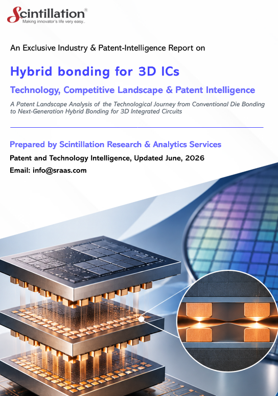
Hybrid Bonding for 3D ICs

  • Home
  • Hybrid Bonding for 3D ICs
Patent Landscape Analysis  ·  Advanced Semiconductor Packaging Series

Stacking Chips Without Solder: How Hybrid Bonding for 3D ICs Is Redefining Semiconductor Integration

A data-grounded look at who is innovating, where intellectual-property activity is concentrated, and what it means for advanced packaging, commercialization, and IP strategy.

Wafer-to-WaferFull-wafer stacking
Die-to-WaferKnown-good-die stacking
Cu-to-CuFine-pitch interconnects
PatentLandscape & whitespace

Report details

Hybrid Bonding for 3D ICs — Patent Landscape Study Report

PublisherScintillation Research
TechnologyHybrid Bonding for 3D ICs
Focus areaAdvanced packaging and high-density chip stacking
Key segmentsW2W, D2W, Cu-Cu, Dielectric Bonding
Coverage8-part landscape study
AudienceIP, Licensing, R&D, Investment
Purpose of the report

A next-generation semiconductor packaging technology

This report explores the emergence of hybrid bonding for 3D ICs as a next-generation semiconductor packaging technology that enables ultra-fine-pitch, high-density vertical interconnects between stacked dies and wafers. It examines the technology's technical foundations, manufacturing approaches, commercial applications, and evolving patent landscape, providing insight into who is innovating, where intellectual-property activity is concentrated, and what these trends mean for advanced packaging, commercialization, and IP strategy.

The report covers key hybrid-bonding technologies, leading assignees, patent-filing trends, technology evolution, applications in 3D ICs and advanced memory, competitive dynamics, whitespace opportunities, and the future outlook for high-density chip stacking, heterogeneous integration, and next-generation semiconductor packaging.

Who will benefit from this report

Built for everyone shaping the future of 3D integration

Each audience gets a clear view of the landscape and what to do with it.

01
Patent Attorneys, Agents & IP Analysts
A structured overview of the hybrid-bonding landscape, including key assignees, patent-filing trends, jurisdictions, technology segments, and emerging innovations, supporting prosecution, freedom-to-operate (FTO), invalidity, and portfolio-development activities.
02
Licensing & Business Development Professionals
Insights into foundational and emerging hybrid-bonding patent portfolios, helping identify potential licensing opportunities, collaboration targets, and commercially significant technology owners across advanced semiconductor packaging.
03
In-House IP & R&D Leaders
Competitive intelligence on hybrid bonding, wafer-to-wafer and die-to-wafer integration, fine-pitch interconnects, and 3D IC manufacturing trends to support strategic planning, technology development, and packaging roadmaps.
04
Investors & Market Analysts
An evidence-based view of innovation activity, commercialization trends, leading assignees, technology adoption, and emerging opportunities within the rapidly evolving 3D IC and advanced semiconductor packaging ecosystem.
05
Semiconductor, Foundry, OSAT & Equipment Companies
Insights into key technology domains, including wafer-to-wafer and die-to-wafer hybrid bonding, copper-to-copper interconnects, dielectric bonding, surface preparation, alignment, bonding processes, thermal management, and high-density 3D integration.
06
Academic Institutions & Semiconductor Research Organizations
Benchmarking information on leading research groups, emerging hybrid-bonding technologies, technology-development pathways, and potential partnership opportunities within the advanced packaging and 3D IC ecosystem.
Introduction

When 2D scaling slows, the chip goes vertical

As performance gains from shrinking transistors become harder and costlier to achieve, the industry is increasingly stacking chips vertically to deliver more bandwidth, density, and functionality in less area. Conventional 3D integration relies on solder micro-bumps and thermocompression bonding to connect stacked dies, but these approaches are limited by bump pitch, bridging risk, underfill requirements, added thickness, and higher electrical and thermal resistance. Hybrid bonding addresses these constraints by directly joining dielectric surfaces and embedded copper pads, without solder, to form permanent electrical and mechanical connections at much finer pitches. The approach is powerful but demanding: it requires extremely clean and flat surfaces, precise alignment, tight process control, particle management, and careful thermal and yield management before it can be applied broadly across wafer-to-wafer and die-to-wafer flows.

Report structure

Table of contents

Twelve chapters, from hybrid bonding fundamentals to patent landscape intelligence. Click any chapter to expand.

—Key findings on hybrid bonding for 3D ICs, leading assignees, filing trends, and strategic implications
—Who Will Benefit from This Report
3.1Limitations of Conventional 3D IC Bonding Technologies
4.1Challenges Addressed by Hybrid Bonding for 3D ICs
4.2Key Features of Hybrid Bonding for 3D ICs
4.3Applications of Hybrid Bonding for 3D ICs
—How hybrid bonding has progressed from early research demonstrations toward high-volume manufacturing
—The technical, commercial, and innovation signals that make the field strategically important
—Commercialization pathways, open challenges, and future directions
8.1Methodology & Scope
8.2Interesting Strategic Insights
8.3Assignee Picture
8.4Filing Activity Over Time
8.5Jurisdiction Coverage
8.6Technology Segmentation
8.7Representative Publications Across the Field
8.8Whitespace & Strategic Opportunities
—Stakeholder-specific takeaways for IP teams, licensing professionals, R&D leaders, semiconductor and equipment companies, and investors
—Synthesis of the technical trajectory, innovation dynamics, and strategic implications
—Overview of Scintillation Research and its patent and technology intelligence services
—Legal disclaimer covering information accuracy, IP ownership, and terms of use
Key features

Core capabilities of hybrid bonding for 3D ICs

The properties that make direct copper-to-copper bonding attractive for vertical integration.

Ultra-fine-pitch interconnects
Pad pitches far finer than solder micro-bumps allow, enabling much denser vertical connections.
High interconnect density
Many more die-to-die connections per unit area, supporting higher bandwidth between stacked chips.
Low resistance and capacitance
Short, direct copper connections improve signal integrity and reduce power per bit transferred.
Solderless, underfill-free joints
Dielectric and copper bond directly, removing solder bridging risk and thinning the overall stack.
Improved thermal path
Thinner bond interfaces and direct copper contact help heat move through the stack more effectively.
Wafer-to-wafer and die-to-wafer flows
Flexible integration options, from high-throughput full-wafer stacking to known-good-die assembly.
Challenges addressed

Why conventional 3D bonding is reaching its limits, and what stays hard

What hybrid bonding aims to address, and where the limits are.

01
Pitch limits of solder micro-bumps
Bump size, bridging risk, and reflow behavior restrict how finely and densely dies can be connected
02
Bandwidth, power, and signal integrity
Longer, more resistive interconnects limit bandwidth and raise energy per bit. Direct copper joints offer shorter, lower-loss paths
03
Stack height and thermal resistance
Bumps, underfill, and thicker interfaces add height and impede heat flow as more dies are stacked
04
Process control, yield, and cost
Surface flatness, cleanliness, particle control, and alignment accuracy are demanding, and tooling and yield management remain costly
Applications

Where hybrid bonding for 3D ICs creates value

Use cases where dense, short, low-loss vertical interconnects are a competitive edge.

High-bandwidth and advanced memory stacking
3D NAND and memory-on-logic
CMOS image sensors
Chiplets and heterogeneous integration
AI accelerators and high-performance computing
Stacked cache and logic-on-logic
Photonics, RF, and specialty devices
Patent landscape study

Who is innovating, where, and in which areas

The study covers methodology and scope, strategic insights, the assignee picture, filing activity over time, jurisdiction coverage, technology segmentation across wafer-to-wafer and die-to-wafer bonding, copper-to-copper interconnects, dielectric bonding, surface preparation, alignment, and thermal management, representative publications across the field, and the whitespace and strategic opportunities for new filings and licensing.
Request Your Sample Report Now!

    For a quick demo, schedule a meeting now!

    Shopping Cart (0 items)

    Subscribe to our newsletter

    Sign up to receive latest news, updates, promotions, and special offers delivered directly to your inbox.
    No, thanks