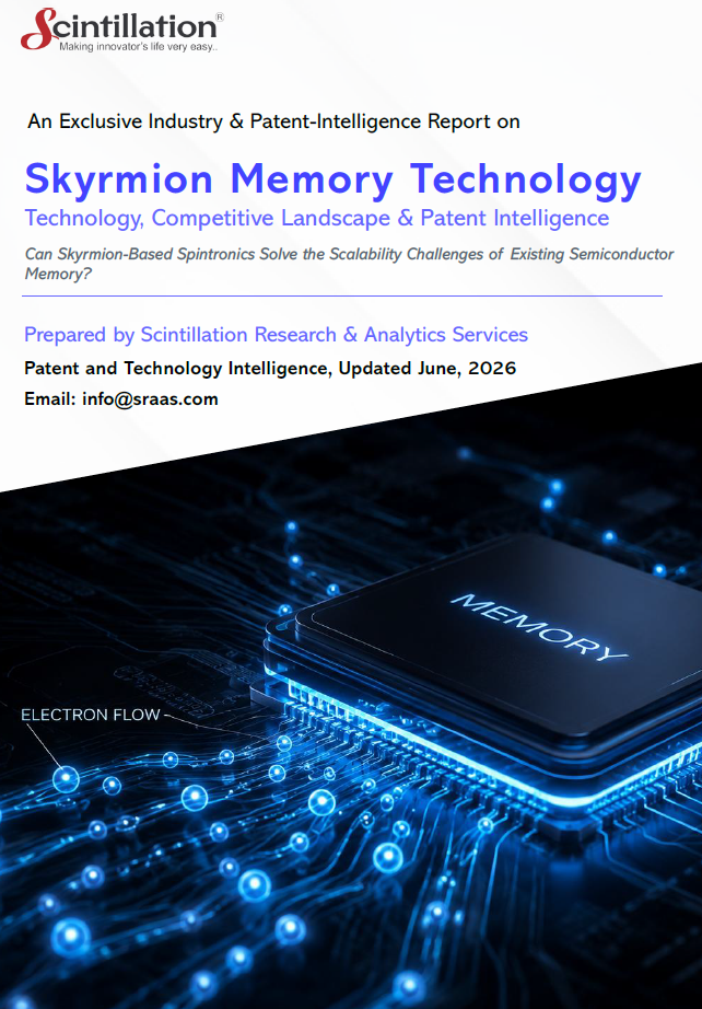
Skyrmions Memory Technology

  • Home
  • Skyrmions Memory Technology
Skyrmion Memory Technology: Can Skyrmion-Based Spintronics Solve the Scalability Challenges of Existing Semiconductor Memory? | Scintillation Research
Patent Intelligence Report  ·  Spintronics & Next-Gen Memory Series

Skyrmion Memory Technology: Can Skyrmion-Based Spintronics Solve the Scalability Challenges of Existing Semiconductor Memory?

A data-grounded look at who is filing, where innovation is concentrated, and why skyrmion-based spintronics is emerging as a leading candidate for ultra-low-power, high-density memory.

A comprehensive technology and patent intelligence analysis of Skyrmion Memory Technology — examining skyrmion racetrack memory, skyrmion creation, manipulation and detection mechanisms, the skyrmion Hall effect, material engineering approaches, and fabrication pathways enabling next-generation, energy-efficient spintronic computing systems.

Racetrack MemorySkyrmion-based data storage
1000xLower power vs. commercial memory
Topological StabilityRobust magnetic structures
PatentLandscape & whitespace analysis

Report details

Skyrmion Memory Technology — Technology & Patent Intelligence Report

Publisher Scintillation Research
Technology Skyrmion Memory Technology
Focus area Spintronics & Next-Gen Memory
Key segments Racetrack Memory, Nucleation, Detection
IP coverage Patent landscape study
Applications Memory, AI Hardware, Edge Computing
Audience IP, R&D, Strategy, Investment
Skyrmion Topological magnetic whirl
1000x Lower power vs. commercial memory
Racetrack Domain-wall memory architecture
IP Patent landscape study
Topological Inherent structural stability
Introduction

When conventional semiconductor memory can no longer meet the scalability and energy demands of next-generation computing

A research team led by the Agency for Science, Technology and Research (A*STAR) in partnership with the National University of Singapore (NUS) has created an innovative microelectronic device that can potentially function as a sustainable, high-performance "bit-switch." This paves the way for future computing technologies to process data much faster while using significantly less energy.

By harnessing tiny, stable and speedy magnetic whirls called skyrmions, the device can operate using 1,000 times less power than commercial memory technologies. This discovery was reported in the journal Nature.

Solitonic magnetic excitations such as domain walls and, specifically, skyrmions enable the possibility of compact, high-density, ultrafast, all-electronic, low-energy devices, which is the basis for the emerging area of skyrmionics. The topological winding of skyrmion spins affects their overall lifetime, energetics, and dynamical behaviour. This report discusses skyrmionics in the context of the present-day solid-state memory landscape, and shows how their size, stability, and mobility can be controlled by material engineering, as well as how they can be nucleated and detected.

Report structure

Table of contents

Ten chapters connecting skyrmion memory's technical foundations to patent landscape intelligence and commercialization strategy. Click any chapter to expand.

Condensed findings on skyrmion memory technology, patent filing trends, assignee dynamics, and strategic implications for spintronics IP
Who Will Benefit from This Report — spintronics researchers, semiconductor strategists, IP counsel, academic institutions, and technology investors tracking next-generation magnetic memory
3.1 Challenges in Conventional Memory Technology — physical scaling limits, power consumption, density constraints, and reliability limitations of existing semiconductor memory architectures
Structural Components of Skyrmion Memory Technology — magnetic thin-film racetracks, skyrmion nucleation sites, spin-current manipulation layers, and detection junctions
4.1 Key Features — ultra-low power operation, high data density, topological stability, and fast current-driven motion
4.2 Problems Skyrmion Memory Technology Aims to Solve — power consumption, density scaling limits, and reliability constraints of conventional memory
4.3 Potential Applications — racetrack memory, AI hardware accelerators, edge computing, and energy-efficient data storage systems
Conventional Memory Technology vs Skyrmion Memory Technology — comparative analysis of power consumption, density, stability, and switching speed
Skyrmion memory deployment roadmap, technological readiness assessment, fabrication scalability, and near-term commercialization opportunities
6.1 Methodology & Scope — patent database coverage, search strategy, classification framework, and analytical approach for skyrmion memory IP
6.2 Assignee Picture — leading filers across semiconductor manufacturers, research institutions, and academic consortia, with notable assignee profiles
6.3 Filing Activity Over Time — trend analysis identifying R&D acceleration and IP maturity signals across skyrmion memory technology domains
6.4 Jurisdiction Coverage — USPTO, CNIPA, KIPO, JPO, EPO, and WIPO distributions across the skyrmion memory patent landscape
6.5 Technology Segmentation — patents mapped to racetrack memory, nucleation and creation mechanisms, manipulation and motion control, and detection techniques
6.6 Foundational Anchor Patents — core IP defining the skyrmion memory landscape and their strategic competitive significance
6.7 Whitespace & Strategic Opportunities — underprotected technology domains and emerging filing opportunities across the skyrmion memory IP ecosystem
Stakeholder-specific takeaways for spintronics researchers, semiconductor strategists, IP counsel, and technology investors
Synthesis of skyrmion memory's technical trajectory, IP landscape dynamics, and strategic implications for next-generation spintronic memory commercialization
Publisher profile, research methodology, and service overview — patent analytics, technology scouting, competitive intelligence, and strategic research across spintronics domains
Full legal disclaimer covering information accuracy, IP ownership, and terms of use for this intelligence report
Inside Skyrmion Memory Technology

Structural components & key features

Skyrmion memory stores information not as electrical charge but as the position of topologically stable, nanoscale magnetic whirls within a thin-film racetrack — enabling current-driven data movement with dramatically lower energy requirements than conventional charge-based memory.

Skyrmion racetrack memory
Magnetic thin-film nanowires along which skyrmions move under current-driven spin-torque, encoding data as the presence and position of skyrmions along the track.
Skyrmion nucleation & creation mechanisms
Current-injection, spin-orbit torque, and local field methods engineered to reliably generate individual skyrmions at defined positions on demand.
Spin-current manipulation
Spin-polarized current and spin-orbit torque mechanisms used to drive skyrmion motion along the racetrack with precise, controllable velocity.
Detection junctions
Magnetic tunnel junctions and related read-head structures used to detect the presence and position of skyrmions for reliable data readout.
Topological stability
A skyrmion's protected topological winding number gives it inherent resistance to thermal and structural perturbation, supporting robust, non-volatile data retention.
Skyrmion Hall effect mitigation
Material and geometry engineering strategies addressing the transverse drift of skyrmions during current-driven motion, a key obstacle to reliable racetrack operation.
Material engineering for size & mobility control
Tailored magnetic multilayer compositions used to tune skyrmion size, lifetime, and mobility — central to achieving practical device performance.
Ultra-low-power switching architecture
Current-driven, all-electronic switching mechanisms that avoid the energy overhead of conventional charge-based switching, enabling dramatic power reduction.
Challenges addressed

Why conventional semiconductor memory cannot meet next-generation scaling demands

Skyrmion memory directly targets the structural constraints that limit how far conventional charge-based semiconductor memory can continue to scale — while confronting new technical hurdles of its own around drift control and material engineering.

01
Physical scaling limits
Conventional charge-based memory technologies face increasing fabrication difficulty and diminishing returns as device dimensions shrink toward atomic scale. Skyrmions, as nanoscale topological structures, offer an inherently different scaling pathway not bound by the same charge-storage limitations
Scaling limits
02
High power consumption
Charge-based memory switching requires comparatively high current and energy input, a growing constraint as data center and edge-device power budgets tighten. Skyrmion-based switching has demonstrated power consumption roughly 1,000 times lower than commercial memory technologies in research settings
Power consumption
03
Density constraints
Achieving higher storage density with conventional memory requires increasingly precise and costly fabrication processes. Skyrmions' nanoscale size and racetrack architecture offer a path toward substantially higher data density within a compact footprint
Density constraints
04
Skyrmion Hall effect
Current-driven skyrmions tend to drift transversely away from their intended path due to the skyrmion Hall effect, complicating reliable racetrack operation. Material engineering and geometry-based mitigation strategies remain an active area of research to address this drift
Skyrmion Hall effect
05
Material limitations & fabrication complexity
Stabilizing skyrmions at room temperature with the size, lifetime, and mobility characteristics needed for practical devices requires precisely engineered magnetic multilayer materials, and large-scale fabrication of these structures remains technically demanding
Fabrication complexity
Conventional vs skyrmion memory

Conventional memory technology vs skyrmion memory technology

A side-by-side view of how skyrmion-based spintronic memory differs from the charge-based memory architectures that dominate today's semiconductor industry.

Dimension Conventional Memory Technology Skyrmion Memory Technology
Information carrier Electrical charge stored in capacitors or transistors Position of topologically stable magnetic skyrmions
Power consumption Relatively high switching energy per bit Demonstrated reductions of up to 1,000x in research settings
Data density Constrained by charge-storage cell size and leakage Potentially higher density via nanoscale skyrmion size
Stability mechanism Relies on charge retention and refresh cycles (for volatile memory) Inherent topological protection provides structural stability
Switching mechanism Voltage-driven charge transfer Current-driven spin-torque motion along a racetrack
Technology maturity Decades of established fabrication and manufacturing infrastructure Emerging technology with active research into fabrication and room-temperature operation

Download Your Sample Report Now:

    Application areas

    Where skyrmion memory creates emerging computational impact

    Skyrmion memory's power, density, and stability advantages are most compelling in applications where conventional charge-based memory faces fundamental energy, scaling, or footprint constraints.

    Racetrack Memory Systems
    High-density, non-volatile storage architectures leveraging current-driven skyrmion motion along magnetic nanowires
    AI Hardware Accelerators
    Energy-efficient memory architectures supporting the high-throughput, low-power demands of AI training and inference hardware
    Edge Computing
    Power-constrained edge devices benefiting from skyrmion memory's dramatically reduced switching energy requirements
    Neuromorphic Computing
    Brain-inspired computing architectures exploring skyrmion dynamics as an analog for synaptic and neuronal behavior
    Data Center Storage
    High-density, energy-efficient storage solutions addressing the growing power demands of large-scale data centers
    Logic-in-Memory Architectures
    Spintronic computing architectures combining memory and logic functions using skyrmion-based device elements
    Sensor & IoT Devices
    Low-power, compact memory solutions suited to battery-constrained Internet of Things and sensor network applications
    Next-Generation Computing Platforms
    Broader beyond-CMOS computing initiatives drawing on skyrmionics as a candidate technology for future energy-efficient systems
    Patent intelligence

    The skyrmion memory patent landscape

    The patent landscape chapter delivers data-grounded IP intelligence — from methodology and assignee profiling to filing trends, jurisdiction coverage, technology segmentation, anchor patents, and whitespace identification across the full skyrmion memory ecosystem.

    Assignee & filing intelligence
    • Methodology and scope defining the boundaries of skyrmion memory patent analysis
    • Assignee picture and notable profiles — semiconductor manufacturers, research institutions, and academic consortia shaping the skyrmion memory IP landscape
    • Filing activity over time — trend analysis identifying R&D acceleration points and IP maturity signals across skyrmion memory technology segments
    • Jurisdiction coverage — USPTO, CNIPA, KIPO, JPO, EPO, and WIPO distributions across the skyrmion memory patent corpus
    Technology & strategic analysis
    • Technology segmentation — racetrack memory, nucleation and creation mechanisms, manipulation and motion control, and detection techniques
    • Foundational anchor patents — core IP defining the skyrmion memory landscape and their strategic competitive significance
    • Whitespace & strategic opportunities — underprotected technology domains and emerging skyrmion memory filing and licensing opportunities
    • Strategic implications for freedom-to-operate, partnership, and research-collaboration decisions across the skyrmion memory ecosystem
    Who will benefit

    Who should read this report

    Spintronics & Magnetic Materials Researchers
    Researchers designing skyrmion nucleation, manipulation, and detection mechanisms, and engineering magnetic materials for stable room-temperature skyrmion behavior.
    Semiconductor & Memory Strategists
    Technology strategists evaluating skyrmion memory as a candidate beyond-CMOS architecture and assessing technological readiness against conventional memory roadmaps.
    IP Counsel & Patent Teams
    Attorneys and patent professionals assessing portfolio positioning, whitespace, freedom-to-operate, and filing strategy across racetrack memory, nucleation, and detection technologies.
    Academic & Government Research Institutions
    Research organizations and government-funded initiatives tracking skyrmionics research direction and identifying collaboration and funding opportunities.
    Technology Investors
    Investment professionals tracking the spintronics and next-generation memory ecosystem, the skyrmion memory IP landscape, and emerging companies in magnetic computing.
    R&D Strategists & Industry Analysts
    Researchers and consultants mapping the competitive skyrmion memory landscape across semiconductor manufacturers, research institutions, and academic consortia driving adoption.
    Technology & Patent Intelligence · Scintillation Research

    Understand who is building the IP foundation for skyrmion-based spintronic memory

    Get the complete technology and patent intelligence report on Skyrmion Memory Technology — from racetrack memory architectures and nucleation mechanisms to the patent landscape revealing who is filing, where innovation is concentrated, and why skyrmion-based spintronics is emerging as a leading candidate for ultra-low-power, high-density memory.

    Scintillation Research · Skyrmion Memory Technology · Patent Intelligence Series

    For a quick demo, schedule a meeting now!

    Service Demo Booking
    About

    About Scintillation Research

    Scintillation Research & Analytics Services is a specialized intellectual property and technology intelligence firm delivering patent analytics, technology scouting, competitive intelligence, and strategic research services.

    Through comprehensive patent and technology intelligence reports, we help organizations understand emerging innovations, identify market opportunities, monitor competitors, and make data-driven decisions across rapidly evolving technology domains. Our reports are designed for professionals at the intersection of technology strategy, IP management, and competitive intelligence.

    Shopping Cart (0 items)

    Subscribe to our newsletter

    Sign up to receive latest news, updates, promotions, and special offers delivered directly to your inbox.
    No, thanks
    Select your currency