
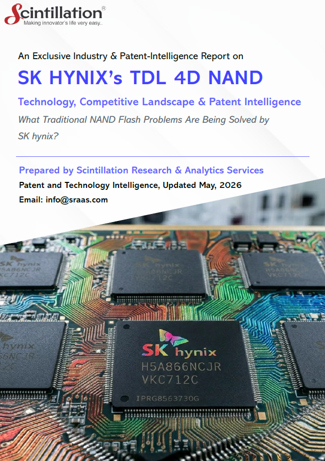
SK Hynix 321-Layer TLC
4D NAND Technology
A comprehensive technology and patent intelligence analysis of SK Hynix's most advanced next-generation flash memory platform — examining ultra-high-layer stacking, 4D NAND architecture, performance innovations, and the evolving intellectual property landscape across AI infrastructure, enterprise SSDs, and hyperscale data centers.
Report details
SK Hynix 321-Layer TLC 4D NAND — Technology & Patent Intelligence
Why SK Hynix's 321-layer 4D NAND matters
The global semiconductor memory industry is rapidly evolving as demand increases for higher-capacity, faster, and more power-efficient storage technologies across AI, hyperscale data centers, enterprise computing, smartphones, and high-performance consumer electronics.
Modern AI workloads, cloud platforms, and high-resolution digital content require memory solutions capable of delivering higher storage density, faster read/write speeds, lower latency, improved energy efficiency, and greater reliability. However, conventional NAND flash technologies continue to face several technical limitations, including slower I/O performance, limited vertical stacking scalability, higher power consumption, thermal management challenges, and storage density constraints.
To address these challenges, SK Hynix is actively developing its 321-layer TLC 4D NAND technology as one of its most advanced next-generation flash memory platforms. The technology utilizes ultra-high-layer vertical stacking and advanced 4D NAND architectures to significantly improve storage density, performance, and power efficiency while supporting the growing demands of AI-driven and data-intensive computing environments.
Unlike traditional NAND architectures with scaling limitations, SK Hynix's advanced 4D NAND design enables more efficient cell integration and higher memory capacity within compact semiconductor footprints. The technology delivers improved read/write performance, lower energy consumption, higher stacking scalability, and enhanced reliability — making it highly suitable for enterprise SSDs, hyperscale AI infrastructure, mobile devices, and high-performance computing systems.
This report explores the technological foundations of SK Hynix's 321-layer TLC 4D NAND architecture, the key challenges it addresses, recent innovations, manufacturing developments, emerging applications, and the future commercialization potential of advanced NAND flash technology within the global semiconductor memory industry.
Table of contents
Ten chapters covering technical foundations, patent landscape, and commercialization strategy across the full 4D NAND value chain.
Key features & technical innovations
SK Hynix's 321-layer TLC 4D NAND converges ultra-high-layer stacking with next-generation cell architecture — unlocking a new class of storage density, speed, and power efficiency.
Limitations of traditional NAND technology
SK Hynix's 321-layer TLC 4D NAND directly targets five critical constraints that have held back conventional flash memory architectures.
What each chapter covers
Eight substantive chapters connect technical innovation to intellectual-property strategy and commercial positioning across the NAND ecosystem.
Request Your Sample Report Now!
