Why the Entire Tech Industry is Watching TSMC’s A14?

  • Home
  • Why the Entire Tech Industry is Watching TSMC’s A14?
TSMC A14 — Why the Entire Tech Industry is Watching | Scintillation Research
Patent Intelligence Report  ·  Semiconductor Process Series

Why the entire tech industry
is watching TSMC's A14

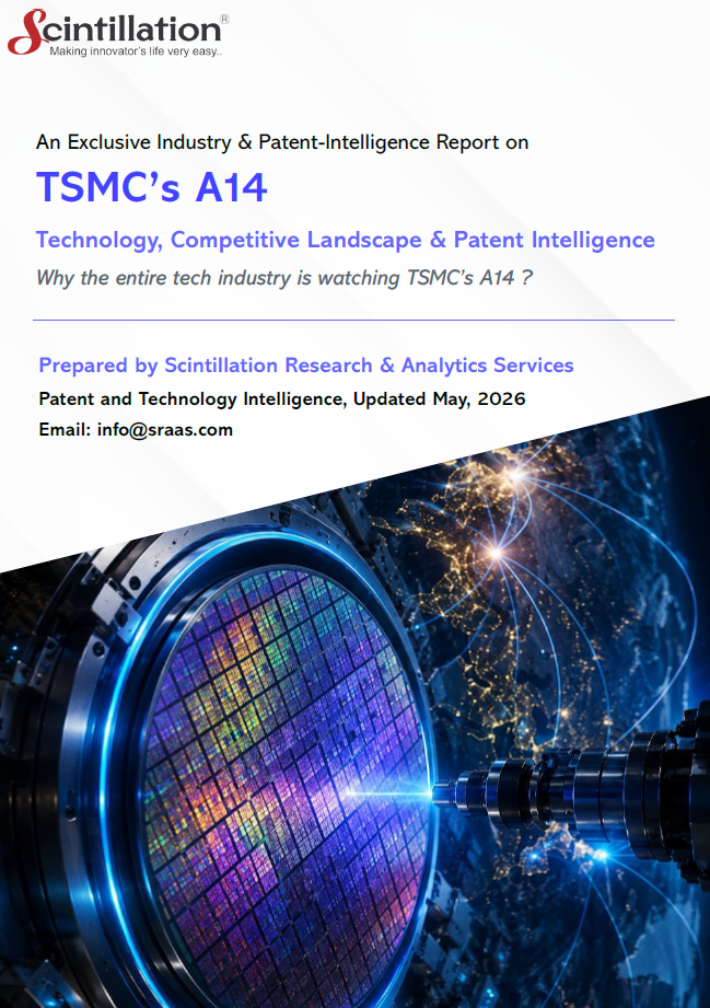
A comprehensive technology and patent intelligence analysis of TSMC's next-generation A14 (1.4nm-class) process — examining second-generation GAA nanosheet transistors, NanoFlex™ Pro architecture, Low-NA EUV strategy, performance benchmarks, and the evolving IP landscape across AI, HPC, smartphones, and edge computing.

+15%Speed vs N2 (same power)
−30%Power vs N2 (same speed)
+20%Logic density improvement
2028Mass production target

Report details

TSMC A14 — Technology & Patent Intelligence Report

Publisher Scintillation Research
Process node A14 (1.4nm-class)
Transistor architecture 2nd-gen GAA Nanosheet
Key feature NanoFlex™ Pro
IP coverage Patent landscape + whitespace
Mass production 2028
Audience IP, R&D, Strategy, Investment
1.4nm Process class
+15% Speed gain vs N2
−30% Power reduction
+20% Logic density
GAA 2nd-gen nanosheet
2028 Production target
Introduction

The semiconductor race to 1.4nm

The global semiconductor industry plays a critical role in enabling modern digital technologies — from artificial intelligence and high-performance computing to cloud infrastructure, smartphones, and autonomous systems.

Continuous advancements in semiconductor manufacturing are essential for improving computing performance, reducing power consumption, increasing transistor density, and supporting the growing demand for intelligent and data-intensive applications. As the industry moves toward smaller process nodes and more advanced transistor architectures, semiconductor companies are focusing on next-generation fabrication technologies capable of sustaining Moore's Law and meeting future computational requirements.

TSMC, the world's leading semiconductor foundry, has introduced its next-generation A14 (1.4nm-class) process technology as part of its continued advancement in semiconductor manufacturing. The A14 process builds upon TSMC's earlier N2 and A16 process nodes and introduces second-generation Gate-All-Around (GAA) nanosheet transistor architecture. GAA transistors provide superior electrostatic control compared to traditional FinFET designs, allowing semiconductor devices to operate at lower voltages while improving switching efficiency and reducing power leakage.

Another major feature of the A14 node is NanoFlex™ Pro technology — an enhanced design-technology co-optimization (DTCO) platform that allows chip designers greater flexibility in balancing power, performance, and chip area. TSMC's strategy also emphasizes manufacturing stability and cost efficiency by continuing to use advanced Low-NA EUV lithography systems instead of immediately transitioning to High-NA EUV, intending to improve yield maturity while maintaining competitive scaling advantages.

This report explores the technological foundations of TSMC's A14 process, the challenges it addresses, its key innovations, the patent landscape, and its commercialization potential across the global semiconductor ecosystem.

Performance benchmarks

A14 vs TSMC's prior process nodes

A14 delivers measurable improvements across speed, power, and density compared to the N2 baseline — repositioning what is achievable at advanced process nodes.

Metric N2 (baseline) A16 A14 A14 improvement
Speed (same power) Baseline Incremental gain Up to +15% +15% vs N2
Power (same speed) Baseline Moderate reduction Up to −30% −30% vs N2
Logic density Baseline Incremental gain +20% >20% improvement
Transistor architecture FinFET GAA 1st-gen GAA 2nd-gen nanosheet Superior electrostatic control
Design flexibility NanoFlex™ NanoFlex™ enhanced NanoFlex™ Pro DTCO co-optimization
Lithography EUV Low-NA EUV Low-NA EUV Yield-optimized strategy
Mass production 2025 2026 2028 On roadmap
Report structure

Table of contents

Ten chapters covering technical foundations, patent landscape, and commercialization strategy. Click any chapter to expand its sections.

Condensed findings and key takeaways on TSMC's A14 technology and its patent and commercial implications
2.1 Who Will Benefit from This Report — R&D strategists, IP counsel, investors, chip designers, and industry analysts
3.1 Challenges in the Semiconductor Industry — Moore's Law pressures, power walls, leakage, and density scaling constraints
4.1 Key Features — 2nd-gen GAA nanosheet transistors, NanoFlex™ Pro, Low-NA EUV lithography, performance specifications
4.2 Problems TSMC's A14 Aims to Solve — power walls, density ceilings, leakage, design-technology co-optimization gaps
4.3 Potential Applications — AI accelerators, HPC chips, flagship smartphones, edge AI, and advanced consumer electronics
Technology roadmap, 2028 production ramp, foundry customer adoption, ecosystem readiness, and market impact analysis
6.1 Methodology & Scope — patent database coverage, search strategy, and classification framework
6.2 Who Is Filing — foundries, fabless designers, equipment makers, materials suppliers, and research institutions
6.3 Filing Activity Over Time — trend analysis identifying acceleration points and technology maturity signals
6.4 Jurisdiction Coverage — USPTO, TIPO, KIPO, CNIPA, EPO, WIPO and regional patent office distributions
6.5 Technology Segmentation — how patents map to GAA transistors, EUV patterning, interconnects, and DTCO
6.6 Legal Status Snapshot — granted, pending, expired, and lapsed portfolio breakdown
6.7 Representative Filings — notable patents and claims shaping the A14 IP landscape
6.8 Whitespace & Strategic Opportunities — unprotected technology areas representing filing and competitive positioning opportunities
Stakeholder-specific takeaways for chip designers, IP counsel, R&D teams, business development, and investors
Synthesis of findings on TSMC A14's technical trajectory, IP landscape, and strategic implications for the semiconductor industry
Publisher profile, research methodology, and approach to technology and patent intelligence analysis
Full legal disclaimer covering information accuracy, IP ownership, and terms of use for this intelligence report
Inside A14 Technology

Key features & technical innovations

A14 combines second-generation GAA nanosheet transistors, NanoFlex™ Pro DTCO, and a refined Low-NA EUV strategy to deliver the semiconductor industry's next performance milestone.

2nd-gen GAA nanosheet transistors
Superior electrostatic gate control over all four sides of the channel — reducing leakage, enabling lower operating voltages and higher switching efficiency.
NanoFlex™ Pro technology
Enhanced design-technology co-optimization (DTCO) platform giving chip designers greater flexibility to balance power, performance, and area for each design target.
Low-NA EUV lithography
Continued use of advanced Low-NA EUV systems to optimize yield maturity and cost efficiency while maintaining competitive scaling — deferring High-NA transition.
+15% speed at same power
Measured against TSMC's N2 node — significant performance headroom for next-generation AI accelerators and high-frequency mobile processors.
−30% power at same speed
Critical for battery-constrained mobile devices and thermally-limited data center deployments seeking higher compute density per watt.
>20% logic density gain
More transistors per mm² enables smaller die sizes, higher integration of complex SoC designs, and greater cost efficiency at volume production.
N2 / A16 process continuity
A14 builds on TSMC's established N2 and A16 process infrastructure, reducing EDA tool migration risk and supporting reuse of prior-generation IP blocks.
AI & HPC optimized
Architecture tuned for the power-performance-area requirements of AI training clusters, inference accelerators, and next-generation HPC processors.
Challenges addressed

Limitations A14 is designed to overcome

The semiconductor industry faces compounding physical and engineering constraints as process nodes shrink. A14 directly targets each of these barriers.
01
FinFET electrostatic scaling limits
At sub-2nm nodes, FinFET gate control degrades due to short-channel effects. GAA nanosheet architecture wraps the gate fully around the channel, restoring electrostatic control
Architecture
02
Power wall and thermal density
Conventional scaling increases power density, creating thermal management challenges. A14's −30% power reduction eases thermal budgets in mobile, edge, and data center deployments
Power
03
Transistor leakage at advanced nodes
Gate leakage and sub-threshold current increase at smaller nodes. GAA's superior gate-channel coupling suppresses leakage, enabling lower standby power consumption
Efficiency
04
Design flexibility vs density tradeoffs
Prior DTCO platforms constrained designers. NanoFlex™ Pro decouples power-performance-area optimization, enabling customized tuning for AI, mobile, and HPC use cases simultaneously
Design
05
High-NA EUV yield and cost risk
Immediate adoption of High-NA EUV carries immature yield and capital cost risks. TSMC's Low-NA EUV strategy for A14 prioritizes yield stability and production cost control through 2028
Manufacturing

Download Your Sample Report Now:

    Application areas

    Target application verticals

    A14's performance, power, and density profile makes it particularly well-suited for the most demanding semiconductor applications across AI, compute, and connectivity.

    AI Accelerators
    Training and inference chips for large language models and frontier AI systems
    High-Performance Computing
    Scientific simulation, financial modeling, weather forecasting processors
    Flagship Smartphones
    Next-generation mobile SoCs for Apple, Qualcomm, MediaTek, and Samsung
    Edge Computing
    On-device AI inference, intelligent sensors, and real-time edge processing
    Hyperscale Data Centers
    Custom silicon for cloud workloads, networking ASICs, and DPUs
    Autonomous Vehicles
    ADAS processors, sensor fusion chips, and vehicle compute platforms
    Advanced Consumer Electronics
    AR/VR headsets, gaming hardware, and next-gen personal compute devices
    5G / 6G Networking
    Baseband processors, RF front-ends, and mmWave radio infrastructure
    Patent intelligence

    The A14 patent landscape — an 8-part analysis

    The patent landscape chapter delivers a structured breakdown of the A14-era IP environment — from filing trends and assignee benchmarking to whitespace identification and representative claim analysis.

    Filing & assignee intelligence
    • Methodology and patent database scope defining the search universe for 1.4nm-class process technology
    • Who is filing — foundries, fabless chip designers, EDA vendors, lithography equipment makers, and materials suppliers
    • Filing activity over time — trend analysis revealing A14-era acceleration and technology maturity signals
    • Jurisdiction coverage — USPTO, TIPO, KIPO, CNIPA, EPO, WIPO, and key regional patent offices
    Technology & strategic analysis
    • Technology segmentation — patents mapped to GAA transistors, EUV patterning, interconnects, DTCO, and NanoFlex™ Pro
    • Legal status snapshot — granted, pending, expired, and lapsed portfolio breakdown by assignee and domain
    • Representative filings — notable patents and claims defining the current A14 IP landscape
    • Whitespace & strategic opportunities — unprotected technology areas representing filing and competitive positioning opportunities
    Purpose & audience

    Built for IP strategy and competitive positioning

    This report connects the technical foundations of TSMC's A14 process to the evolving intellectual-property landscape — enabling readers to understand not only the architecture and performance innovations, but also the strategic implications for patenting, licensing, competitive benchmarking, and investment decisions across the global semiconductor manufacturing industry.

    Who will benefit

    Who should read this report

    Chip Designers & SoC Teams
    Engineers evaluating A14 process capabilities, NanoFlex™ Pro design rules, and timing for tape-out planning on TSMC's 1.4nm node.
    IP Counsel & Patent Teams
    Attorneys and patent professionals assessing portfolio positioning, whitespace, freedom-to-operate, and filing strategy around GAA and DTCO innovations.
    R&D Strategists
    Technical teams tracking GAA nanosheet architecture, EUV lithography strategy, and the process node roadmap through the 2nm and 1nm era.
    Technology Investors
    Investment professionals tracking the semiconductor manufacturing ecosystem, TSMC competitive positioning, and IP dynamics at advanced nodes.
    Business Development
    Licensing, partnership, and M&A teams evaluating IP portfolios in the advanced process node ecosystem including EDA, materials, and equipment.
    Semiconductor Industry Analysts
    Researchers and consultants mapping the competitive landscape across TSMC, Samsung Foundry, Intel Foundry, and emerging advanced node players.
    Technology & Patent Intelligence · Scintillation Research

    Understand why A14 will define the next era of computing

    Get the complete technology and patent intelligence report on TSMC's A14 process — from GAA nanosheet architecture to the patent landscape shaping the 1.4nm ecosystem.

    Scintillation Research · TSMC A14 · Patent Intelligence Series

    For a quick demo, schedule a meeting now!

    Service Demo Booking
    About

    About Scintillation Research

    Scintillation Research & Analytics Services is a specialized intellectual property and technology intelligence firm delivering patent analytics, technology scouting, competitive intelligence, and strategic research services. Through comprehensive patent and technology intelligence reports, we help organizations understand emerging innovations, identify market opportunities, monitor competitors, and make data-driven decisions across rapidly evolving technology domains.

    Shopping Cart (0 items)

    Subscribe to our newsletter

    Sign up to receive latest news, updates, promotions, and special offers delivered directly to your inbox.
    No, thanks
    Select your currency