Can Glass Substrate Packaging Eliminate Signal Loss and Crosstalk in Advanced Semiconductor Systems?

  • Home
  • Can Glass Substrate Packaging Eliminate Signal Loss and Crosstalk in Advanced Semiconductor Systems?
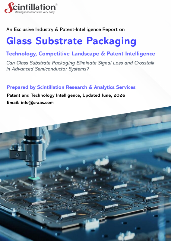
Glass Substrate Packaging: Eliminating Signal Loss and Crosstalk in Advanced Semiconductor Systems | Scintillation Research
Patent Intelligence Report  ·  Advanced Packaging Series

Can Glass Substrate Packaging Eliminate Signal Loss and Crosstalk in Advanced Semiconductor Systems?

A data-grounded look at who is filing, where innovation is concentrated, and why glass substrates are becoming strategically critical for next-generation semiconductor packaging and heterogeneous system integration.

A comprehensive technology and patent intelligence analysis of glass substrate packaging for advanced semiconductor systems — examining dimensional stability, ultra-flat surface characteristics, low coefficient of thermal expansion (CTE), fine-pitch interconnect density, through-glass vias (TGV), electrical performance, mechanical reliability, and large-format substrate architectures enabling next-generation chiplet integration and heterogeneous system-in-package platforms.

Glass CoreNext-gen substrate platform
Low CTEDimensional stability
TGVThrough-glass via interconnects
PatentLandscape & whitespace analysis

Report details

Glass Substrate Packaging — Technology & Patent Intelligence Report

Publisher Scintillation Research
Technology Glass Substrate Packaging
Focus area Advanced Semiconductor Packaging
Key segments TGV, Fine-Pitch RDL, Chiplet, SiP
IP coverage Patent landscape study
Applications AI, HPC, Data Centers, Networking, Auto
Audience IP, R&D, Strategy, Investment
GSP Glass substrate packaging
CTE Low thermal expansion
TGV Through-glass via interconnects
IP Patent landscape study
SiP System-in-package integration
Introduction

When organic substrates and PCB-based packaging can no longer meet next-generation semiconductor demands

The semiconductor industry globally is undergoing a major technological transition, driven by increasing demand for high-performance computing, artificial intelligence (AI), data centers, advanced networking, automotive electronics, and heterogeneous system integration. Advanced electronic devices demand semiconductor packages that sustain higher transistor densities while also supporting faster data transfer rates, increased power delivery and better thermal management capabilities, all while maintaining compact form factors and being scalable to high-yield manufacturing.

However, traditional organic substrates and printed circuit board (PCB)-based packaging technologies continue to face several challenges, including dimensional instability, limited interconnect density, signal-integrity degradation, warpage issues, and constraints in supporting next-generation chip architectures.

To address these challenges, the semiconductor industry is actively working on advanced package technology through R&D. The packaging playbook used by industry leaders has been to explore novel glass substrate-based packaging solutions to improve electrical performance, mechanical stability, thermal efficiency and integration density. Glass substrate technology is widely considered a promising next-generation packaging platform due to its excellent dimensional stability, ultra-flat surface characteristics, low coefficient of thermal expansion (CTE), superior electrical properties, and capability to support fine-pitch interconnects and large-format package architectures.

There is an industry-level strategy focused on supporting next-generation semiconductor systems that meet the computational requirements of artificial intelligence (AI), high-performance computing (HPC), cloud infrastructure, advanced communications, and intelligent edge devices. A lot of work is being done to develop packaging platforms by integrating advanced substrate materials and high-density interconnect technologies into energy-efficient, reliable packages that are fast to manufacture at scale and cost-effective. Over the last few years, glass substrates have been targeted as a major enabler for chiplet architectures, heterogeneous integration, and solutions beyond advanced packaging / system-in-package (SiP) technology.

This report explores glass substrate packaging technology and evaluates how it can help address key challenges in the current semiconductor packaging ecosystem. It also examines the potential impact of glass substrates on future semiconductor manufacturing, advanced packaging strategies, and the broader electronics industry.

Report structure

Table of contents

Ten chapters connecting glass substrate packaging's technical foundations to patent landscape intelligence and commercialization strategy. Click any chapter to expand.

Condensed findings on glass substrate packaging technology, patent filing trends, assignee dynamics, and strategic implications for advanced semiconductor packaging IP
2.1 Who Will Benefit from This Report — packaging engineers, materials scientists, IP counsel, semiconductor strategists, and technology investors tracking next-generation substrate platforms
3.1 Challenges in Advanced Substrate Packaging Technologies — dimensional instability, limited interconnect density, signal-integrity degradation, warpage issues, and constraints in supporting next-generation chip architectures
Structural components — glass core layers, through-glass vias (TGV), fine-pitch redistribution layers, embedded die cavities, and large-format panel architectures
4.1 Key Features — dimensional stability, ultra-flat surface characteristics, low coefficient of thermal expansion, fine-pitch interconnect support, and large-format scalability
4.2 Problems Glass Packaging Aims to Solve — signal loss, crosstalk, warpage, limited interconnect density, and thermal-mechanical reliability limitations of organic substrates
4.3 Potential Applications — AI accelerators, high-performance computing, data centers, advanced networking, automotive electronics, and heterogeneous chiplet platforms
Glass substrate deployment roadmap, manufacturing scalability and yield challenges, standards development, and near-term commercialization opportunities for next-generation semiconductor packaging
6.1 Methodology & Scope — patent database coverage, search strategy, classification framework, and analytical approach for glass substrate packaging IP
6.2 Who Is Filing — leading filers across IDMs, OSAT providers, substrate and materials specialists, and equipment vendors shaping the glass substrate IP landscape
6.3 Filing Activity Over Time — trend analysis identifying R&D acceleration and IP maturity signals across glass substrate technology domains
6.4 Jurisdiction Coverage — USPTO, CNIPA, KIPO, JPO, EPO, and WIPO distributions across the glass substrate patent landscape
6.5 Technology Segmentation — patents mapped to through-glass vias, fine-pitch RDL, glass core materials, embedded die integration, and thermal-mechanical reliability
6.6 Whitespace & Strategic Opportunities — underprotected technology domains and emerging filing opportunities across the glass substrate packaging IP ecosystem
Stakeholder-specific takeaways for packaging engineers, materials scientists, IP counsel, semiconductor strategists, and technology investors
Synthesis of glass substrate packaging's technical trajectory, IP landscape dynamics, and strategic implications for next-generation semiconductor commercialization
Publisher profile, research methodology, and service overview — patent analytics, technology scouting, competitive intelligence, and strategic research across semiconductor and advanced packaging domains
Full legal disclaimer covering information accuracy, IP ownership, and terms of use for this intelligence report
Inside Glass Substrate Packaging

Structural components & key features

Glass substrate packaging replaces organic core materials with engineered glass panels — offering dimensional stability, an ultra-flat surface, and a low coefficient of thermal expansion that together enable finer interconnects and larger package formats than conventional substrates can reliably support.

Glass core substrate layers
Engineered glass panels forming the structural core of the package — offering ultra-flat surfaces, high dimensional stability, and mechanical rigidity not achievable with organic laminate cores.
Through-glass vias (TGV)
Vertical interconnect structures etched or drilled through the glass core, enabling fine-pitch signal and power routing between layers with low electrical loss and tight dimensional tolerance.
Fine-pitch redistribution layers (RDL)
Multi-layer RDL structures built on the ultra-flat glass surface, enabling tighter line/space routing than achievable on warpage-prone organic substrates — critical for high-density chiplet interconnects.
Embedded die & component integration
Cavity and embedding architectures that integrate active dies, passives, and chiplets directly within or atop the glass substrate — supporting heterogeneous system-in-package designs.
Signal integrity & low-loss electrical performance
Low dielectric loss and superior electrical properties of glass relative to organic materials — reducing signal attenuation and crosstalk at high data rates required by advanced computing systems.
Low coefficient of thermal expansion (CTE)
Glass's low and tunable CTE closely matches silicon, reducing warpage and thermal-mechanical stress across temperature cycling — improving reliability for large-format, high-density packages.
Large-format panel architectures
Glass panels manufactured at large rectangular form factors, supporting bigger package sizes and higher interconnect density for multi-chiplet AI and HPC packages than wafer-based formats allow.
Power delivery & thermal management
Integrated power distribution and heat dissipation structures co-designed with the glass substrate to manage the thermal and electrical demands of high-power AI and HPC dies.
Challenges addressed

Why organic substrates and PCB-based packaging cannot meet next-generation demands

Glass substrate packaging directly targets five structural constraints that prevent conventional organic substrates and PCB-based packaging from meeting the signal integrity, density, and reliability requirements of next-generation semiconductor systems — while also confronting new challenges of its own, including fragility, inspection complexity, and a lack of established standards.
01
Signal loss & crosstalk
Organic substrate materials exhibit higher dielectric loss than glass, degrading signal integrity and increasing crosstalk between adjacent interconnects as data rates climb. Glass's superior electrical properties reduce signal attenuation and enable cleaner high-speed data transfer
Signal integrity
02
Dimensional instability & warpage
Organic substrates expand and contract unevenly with temperature, causing warpage that limits achievable interconnect density and package size. Glass's low and tunable coefficient of thermal expansion closely matches silicon, substantially reducing warpage-related yield loss
Dimensional stability
03
Limited interconnect density
The rough surface and dimensional variability of organic substrates constrain how fine a line/space pitch can be reliably manufactured. Glass's ultra-flat surface enables substantially finer-pitch redistribution layers and through-glass vias, supporting higher interconnect density for chiplet architectures
Interconnect density
04
Fragility & mechanical handling
Glass is inherently more brittle than organic laminate, introducing new mechanical handling, cracking, and chipping risks during fabrication and assembly that must be addressed through process and material innovation before glass substrates can be deployed at volume
Mechanical reliability
05
Inspection complexity & lack of standards
Glass substrate manufacturing lacks the decades of established process standards, defect-inspection methodology, and supply-chain maturity that organic substrates benefit from — creating near-term adoption friction that the industry is actively working to resolve through R&D and standardization efforts
Standards & inspection

Download Your Sample Report Now:

    Application areas

    Where glass substrate packaging creates critical performance impact

    Glass substrate packaging's signal integrity, density, and reliability advantages are most compelling in applications where data rates, package size, and heterogeneous integration complexity push organic substrates beyond their electrical and mechanical limits.

    AI Accelerators
    GPU, TPU, and AI ASIC packaging requiring low signal loss and high interconnect density at large die areas where organic substrate limits become prohibitive
    High-Performance Computing
    HPC platforms where interconnect density, signal integrity, and packaging reliability directly determine achievable system performance and scalability
    Data Centers & Cloud Infrastructure
    Hyperscale server and accelerator packaging where glass substrates' reliability and density advantages translate to lower failure rates and better performance at scale
    Advanced Networking
    High-speed networking silicon requiring minimal signal loss and crosstalk to support escalating data transfer rates in switches and interconnect modules
    Automotive Electronics
    ADAS and autonomous vehicle compute modules requiring reliable, thermally stable packaging for AI processors and sensor interface dies under automotive qualification standards
    Heterogeneous System Integration
    Multi-die, multi-node chiplet platforms requiring a dimensionally stable, high-density substrate to integrate logic, memory, and I/O dies into a single system-in-package
    Edge & Intelligent Devices
    Power- and space-constrained edge computing platforms benefiting from glass substrates' reliability and integration density in compact form factors
    System-in-Package (SiP) Platforms
    Next-generation SiP architectures using glass substrates as a foundational platform for chiplet integration beyond conventional advanced packaging
    Patent intelligence

    The glass substrate packaging patent landscape

    The patent landscape chapter delivers data-grounded IP intelligence — from methodology and filer profiling to filing trends, jurisdiction coverage, technology segmentation, and whitespace identification across the full glass substrate packaging ecosystem.

    Filing & jurisdiction intelligence
    • Methodology and scope defining the boundaries of glass substrate packaging patent analysis
    • Who is filing — IDMs, OSAT providers, substrate and materials specialists, and equipment vendors shaping the glass substrate IP landscape
    • Filing activity over time — trend analysis identifying R&D acceleration points and IP maturity signals across the technology domain
    • Jurisdiction coverage — USPTO, CNIPA, KIPO, JPO, EPO, and WIPO distributions across the glass substrate patent corpus
    Technology & strategic analysis
    • Technology segmentation — through-glass vias, fine-pitch RDL, glass core materials, embedded die integration, and thermal-mechanical reliability
    • Whitespace & strategic opportunities — underprotected technology domains and emerging glass substrate filing and licensing opportunities
    • Strategic implications for freedom-to-operate, partnership, and supply-chain positioning across the glass substrate ecosystem
    • Signals of competitive intensity and IP maturity heading into anticipated volume production ramp
    Who will benefit

    Who should read this report

    Packaging Engineers & R&D Teams
    Technical teams designing glass core architectures, through-glass via processes, fine-pitch RDL structures, and embedded die integration for next-generation semiconductor packages.
    Materials Scientists
    Researchers developing glass formulations, CTE-tuning approaches, and mechanical-reliability solutions to address fragility and handling challenges in glass substrate manufacturing.
    IP Counsel & Patent Teams
    Attorneys and patent professionals assessing portfolio positioning, whitespace, freedom-to-operate, and filing strategy across glass core, TGV, and fine-pitch interconnect technologies.
    Semiconductor & Packaging Strategists
    Strategy professionals at IDMs, OSAT providers, and substrate manufacturers evaluating glass substrate investment timelines, standards development, and competitive IP positioning.
    Technology Investors
    Investment professionals tracking the advanced packaging ecosystem, the glass substrate IP landscape, and emerging companies in glass core materials and panel-scale processing equipment.
    R&D Strategists & Industry Analysts
    Researchers and consultants mapping the competitive glass substrate packaging landscape across semiconductor companies, materials specialists, and equipment vendors driving adoption.
    Technology & Patent Intelligence · Scintillation Research

    Understand who is building the IP foundation for glass substrate packaging

    Get the complete technology and patent intelligence report on Glass Substrate Packaging — from through-glass vias and fine-pitch interconnects to the patent landscape revealing who is filing, where innovation is concentrated, and why glass substrates are becoming strategically critical for next-generation semiconductor systems.

    Scintillation Research · Glass Substrate Packaging · Patent Intelligence Series

    For a quick demo, schedule a meeting now!

    Service Demo Booking
    About

    About Scintillation Research

    Scintillation Research & Analytics Services is a specialized intellectual property and technology intelligence firm delivering patent analytics, technology scouting, competitive intelligence, and strategic research services.

    Through comprehensive patent and technology intelligence reports, we help organizations understand emerging innovations, identify market opportunities, monitor competitors, and make data-driven decisions across rapidly evolving technology domains. Our reports are designed for professionals at the intersection of technology strategy, IP management, and competitive intelligence.

    Shopping Cart (0 items)

    Subscribe to our newsletter

    Sign up to receive latest news, updates, promotions, and special offers delivered directly to your inbox.
    No, thanks
    Select your currency